Printed circuit board (PCB) layout may be considered sort of an art form by circuit designers, and there is much truth to that. Creating the most reliable, functional, yet cost-effective circuit and finished PCB can be a challenging task, especially in today’s demand for increasingly-complex requirements for compact, light-weight, even flexible boards.
One of the first considerations in the layout of the PCB is size and shape. The end result must accommodate the environment where the board will be installed and utilized, driving the design process. Space considerations may warrant the use of multi-layer or high-density interconnect (HDI) designs. Some projects call for specialized board shapes and weight limitations, making layout particularly challenging.
Although this may not be a major consideration when designing the initial circuit for functionality, in such cases as prototype design, it becomes a higher priority when laying out PCBs for production manufacturing.
Consider your fabricator in the PCB layout phase. Not all manufacturers can produce higher-count multi-layer boards or HDI PCBs. PCB layout design that calls for technologies such as flex or flex-rigid construction for the most part will need to be vetted with the proposed vendor, to ensure the layout design and material requirements can be accommodated.
Special requirements such as a need to incorporate lead-free construction or otherwise avoid potentially hazardous materials can be key points in making layout and construction decisions.
Technical PCB Layout Issues
Other more technical factors to consider in PCB layout:
- Trace widths
- Spacing between traces
- Tolerances for electrical factors that may influence board functionality
- Clearance of traces and components to board edge
Component availability – hard-to-find or specialized components can significantly increase the cost of the final board. Where high numbers of boards are expected to be produced, this can be a major concern, if lower-cost alternatives may be available.
Construction methodology – PCB layout is dependent largely on the physical construction of the boards: through-hole assembly, surface-mount technology (SMT), or a combination of the two. Multi-layer and HDI board designs have grown in use rapidly in recent years, with many specific layout requirements for those technologies.
Importance of PCB Layout
Lack of efficient and accurate layout can result in nearly infinite problems, among them:
- Electromagnetic interference from conflicting components or trace placement
- Conflicts from components on opposite sides of the board
- Rework by designer and delays in manufacturing
- Limited board functionality
- Total board failure
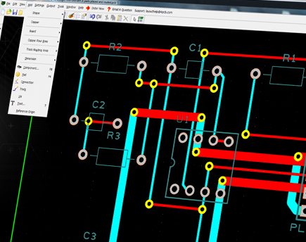
Solving Many PCB Layout Problems
Sophisticated computer aided design (CAD) and computer aided manufacturing (CAM) software systems are now available and in use by most PCB designers and manufacturers. Such specialized programs have many advantages over traditional engineering methods:
- Drag and drop design – place components easily and accurately, then let the software generate the traces for connections. Move or add components easily and instantly.
- Validation of layout – tolerances, compatibility, component placement, and more are verified during design, and prior to releasing the PCB for manufacturing, even for prototypes.
- Reuse – once a layout has been approved and saved, it can be reused as a template for new PCB projects, and utilized by other engineers.
- Efficiency – using such specialized programs can speed development, reduce errors, and result in faster time to market.
- Cost savings – efficiency equates to savings in re-design or manufacturing errors.
- Error detection – basic errors are caught in real time, avoiding defects in manufacturing or delays when fabricators detect them.
- Rule creation – many of these programs support creation of custom rule sets specific to a designer’s purposes. Creating these rules and storing them allows sharing among designers and enhances the functionality of the software.
- Documentation – designs can generate detailed documentation on component use, error reports, design status, version control, and more.
- Generation of manufacturing files – create Gerber files or other formats for the manufacturer quickly and easily, ensuring accurate specifications for fabrication including component placement, via specifications, traces, silk screens, solder masks, and drill files.
Always keep Design for Manufacturing (DFM) in mind in PCB layout and design. The most brilliant and creative PCB layout is of little value if it either cannot be manufactured within the project budget, or is not feasible for manufacturing by the designated fabricator.